| |
|
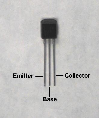
Note that this inserts an emitter follower buffer between
the function generator output and the load.

|
Step 6: |
|
With the scope, measure  .
Sketch the waveform, noting the p-p and average value.
.
Sketch the waveform, noting the p-p and average value.
|
Step 7: |
|
Compute the voltage gain,
 and the offset
 .
.
|
Question 3: |
|
Compute the
average
power
delivered to the load ( )
and dissipated by the transistor (
)
and dissipated by the transistor ( ).
The power rating for the load resistor is 1/4 W
and for the transistor is 625 mW.
Have we exeeded the rating of either component?
).
The power rating for the load resistor is 1/4 W
and for the transistor is 625 mW.
Have we exeeded the rating of either component?
|
Step 8: |
|
Replace the 47 ohm resistor with a 470 ohm resistor.
Measure
and compute the voltage gain and offset.
Are they significantly different from the previous values?
|

